what device converts an analog signal to digital and a digital signal to analog?
Analog-to-Digital and Digital-to-Analog Converters
The world is analog, only signal processing nowadays is digital.The transition between the two domains is done using analog-to-digital (A/D) and digital-to-analog (D/A) converters.
Connecting digital circuitry to sensor devices is elementary if the sensor devices are inherently digital themselves.
Switches, relays, and encoders are easily interfaced with gate circuits due to the on/off nature of their signals.
However, when analog devices are involved, interfacing becomes much more complex.
Hence, we need a way to electronically translate analog signals into digital (binary) quantities, and vice versa.
An analog-to-digital converter, or ADC, performs the quondam task while a digital-to-analog converter, or DAC, performs the latter.
An analog to digital converter (ADC, A/D, or A to D) is a device that converts a continuous physical quantity (usually voltage) to a digital number that represents the quantity'south aamplitude.In block diagram form, it tin be represented equally such:
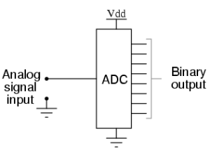
Fig.1
A DAC, on the other manus, inputs a binary number and outputs an analog voltage or current indicate.
In block diagram form, it looks like as below:
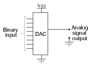
Fig.2
Together, they are often used in digital systems to provide complete interface with analog sensors and output devices for control systems such as those used in automotive engine controls:
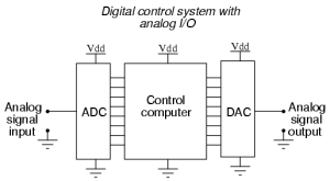
Fig.iii
It is much easier to convert a digital signal into an analog signal than information technology is to do the reverse. Therefore, we will begin with DAC circuitry and then move to ADC circuitry.
Digital to Analog Converter using Binary-Weighted Resistors
A D/A converter using binary-weighted resistors is shown in the effigy below.
In the circuit, the op-amp is connected in the inverting mode.The op-amp can also be connected in the non-inverting way.
The excursion diagram represents a 4-digit converter. Thus, the number of binary inputs is four.
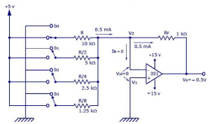
Fig.4
We know that, a four-fleck converter volition have twoiv = 16 combinations of output. Thus, a corresponding 16 outputs of analog will also be present for the binary inputs.
Working
The excursion is basically working as a current to voltage converter.
When b0 is closed:
- It will exist continued direct to the +5V. Thus, voltage across R = 5V.
- So, current through R = 5V/10KΩ = 0.5mA.
- Electric current through feedback resistor, Rf = 0.5mA (Since, Input bias current, I B is negligible).
- Thus, output voltage = -(1KΩ)×(0.5mA) = -0.5V.
When b1 is closed, and b0 is open:
- R/2 will be continued to the positive supply of the +5V.
- Then current through the resistor volition become 5V/5KΩ = 1mA to menstruum through Rf.
- Thus, output voltage also doubles and Output voltage = -(1KΩ)×(1mA)= -1V.
When b0 and b1 are airtight:
- Current through Rf = 1.5mA
- Hence, output voltage = -(1kohm)*(one.5mA) = -i.5V
Thus, co-ordinate to the position (ON/OFF) of the switches (bo-b3), the corresponding "binary-weighted" currents volition be obtained in the input resistor.
The current through Rf will exist the sum of these currents.
This overall current is then converted to its proportional output voltage.
The output volition be maximum if the switches (b0-b3) are closed.
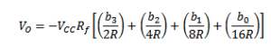
Output voltage equation is given below:
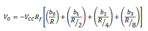
The graph with the analog outputs versus possible combinations of inputs is shown below.
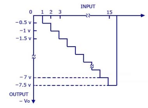
Fig.five
The output is a negative going staircase waveform with 15 steps of -0.5V each.
In practise, due to the variations in the logic High voltage levels, all the steps will non take the same size.
The value of the feedback resistor Rfchanges the size of the steps. Thus, a desired size for a step tin be obtained by connecting the appropriate feedback resistor.
The only condition to look out for is that the maximum output voltage should not exceed the saturation levels of the op-amp.
Disadvantages
If the number of inputs (>iv) or combinations (>16) is more than, the binary-weighted resistors may not be readily available. This is why; R and 2R method is more preferred as it requires merely two sets of precision resistance values.
Digital to Analog Converter with R and 2R Resistors
A D/A converter with R and 2R resistors is shown in the effigy below.
As in the binary-weighted resistors method, the binary inputs are applied past the switches (b0-b3), and the output is proportional to the binary inputs.
Binary inputs tin can exist either in the HIGH (+5V) or Low (0V) country. Let b3 exist the most significant fleck and thus is continued to the +5V and all the other switchs are continued to the ground.
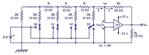
Fig.6
Thus, according to Thevenin's equivalent resistance, R Thursday,
R Th = [{[(2RII2R + R)} II2R] + R}II2R] + R = 2R = 20kOhms.
The resultant circuit is shown beneath.
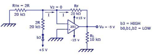
Fig.seven
Graph is given below.
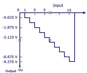
Fig.8
In the figure shown above, the negative input is at virtual ground, therefore the current through R Thursday=0.
Electric current through 2R connected to +5V = 5V/20KΩ = 0.25 mA
The electric current will be the same as that in Rf.
V o = -(20KΩ)*(0.25mA) = -5V.
Output voltage equation is given below:
Wink Analog to Digital Converter
It is as well known asparallel A/D converter and is formed of a series of comparators, each 1 comparing the input betoken to a unique reference voltage.
The comparator outputs connect to the inputs of a priority encoder circuit, which and so produces a binary output.
The following case shows a iii-flake wink ADC circuit:
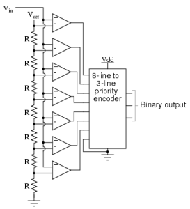
Fig.nine
5ref is a stable reference voltage provided by a precision voltage regulator equally part of the converter circuit, not shown in diagram.
Every bit the analog input voltage exceeds the reference voltage at each comparator, the comparator outputs volition sequentially saturate to a high state.
The priority encoder generates a binary number based on the highest-society active input, ignoring all other active inputs.
When operated, the flash ADC produces an output that looks something like this:
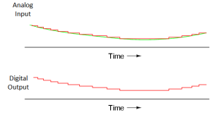
Fig.10
For this item application, a regular priority encoder with all its inherent complexity isn't necessary.
It may exist realized through a set of Exclusive-OR gates, allowing the utilise of a simpler, not-priority encoder every bit shown beneath in Fig.12.
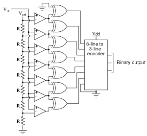
Fig.11
The flash converter is not only the simplest in terms of operational theory, only it is the nigh efficient in terms of speed, being limited merely in comparator and gate propagation delays.
Unfortunately, it is the most component-intensive for any given number of output bits.
The three-bit wink ADC requires seven comparators. A four-scrap version would crave xv comparators. With each boosted output fleck, the number of required comparators doubles.
Considering that 8 bits is generally considered the minimum necessary for any applied ADC (255 comparators needed), the wink methodology quickly shows its weakness.
Digital Ramp Analog to Digital Converter
Information technology is also known as the stairstep-ramp, or just counter A/D converter.
The basic idea of this ADC, is to connect the output of a free-running binary counter to the input of a DAC, so compare the analog output of the DAC with the analog input signal to be digitized and use the comparator's output to tell the counter when to stop counting and reset.
The following schematic shows the basic thought:
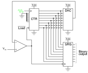
Fig.12
Operation
As the counter counts upward with each clock pulse, the DAC outputs a slightly higher (more positive) voltage.
This voltage is compared against the input voltage by the comparator.
If the input voltage is greater than the DAC output, the comparator'due south output will exist high and the counter will go along counting normally.
Eventually, though, the DAC output will exceed the input voltage, causing the comparator'due south output to go low. This will cause two things to happen:
- first, the high-to-low transition of the comparator's output volition cause the shift register to "load" whatsoever binary count is being output by the counter, thus updating the ADC circuit's output.
- secondly, the counter will receive a low signal on the agile-low LOAD input, causing it to reset to 00000000 on the side by side clock pulse.
The effect of this circuit is to produce a DAC output that ramps up to any level the analog input signal is at, output the binary number corresponding to that level, and start over once again.
The input and output waveform of a Digital Ramp ADC is shown below:
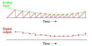
Fig.13
Note that the fourth dimension between the digital output values changes depending on how high the input voltage is.
For low signal levels, the digital outputs are rather shut-spaced. For higher indicate levels, they are spaced further apart in fourth dimension:
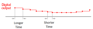
Fig.14
For many ADC applications, this variation in sample fourth dimension would not be acceptable.
This excursion need to count all the way from 0 at the commencement of each count cycle makes for relatively slow sampling of the analog signal, places the digital-ramp ADC at a disadvantage.
Successive Approximation Blazon Analog to Digital Converter
One method of addressing the digital ramp ADC'due south shortcomings is the so-called successive-approximation type ADC.
The only change in this design is a very special counter circuit known every bit a successive-approximation annals.
Instead of counting up in binary sequence, this register counts by trying all values of $.25 starting with the most-meaning bit and finishing at the least-significant bit.
Throughout the count process, the register monitors the comparator's output to see if the binary count is less than or greater than the analog signal input, adjusting the bit values accordingly.
The way the annals counts is identical to the "trial-and-fit" method of decimal-to-binary conversion, whereby unlike values of $.25 are tried from MSB to LSB to become a binary number that equals the original decimal number.
The reward to this counting strategy is much faster results: the DAC output converges on the analog signal input in much larger steps than with the 0-to-full count sequence of a regular counter.
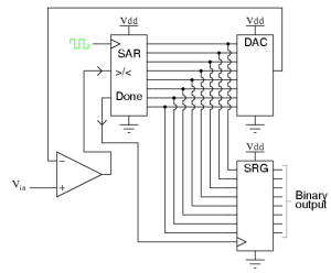
Fig.15
It should be noted that the SAR is more often than not capable of outputting the binary number in series (i bit at a time) format, thus eliminating the need for a shift annals.
Plotted over time, the functioning of a successive-approximation ADC is every bit shown beneath:
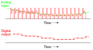
Fig.sixteen
It can be noted that the updates for this ADC occur at regular intervals, unlike the digital ramp ADC circuit.
Source: https://electronicspost.com/analog-to-digital-and-digital-to-analog-converters/
0 Response to "what device converts an analog signal to digital and a digital signal to analog?"
ارسال یک نظر